by Clarence Oxford
Los Angeles CA (SPX) Apr 29, 2026
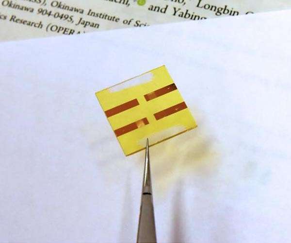
A new study describes a perovskite diode that achieves 26.7% power-conversion efficiency when operated as a solar cell and 31% external quantum efficiency when operated as a light-emitting diode, performance levels that would be considered strong for a device designed to do only one of those things.
Metal-halide perovskites are a class of semiconductor materials named for their distinctive crystal structure that have emerged over the past decade as leading candidates for next-generation solar cells and LEDs. They are relatively inexpensive to produce, can be tuned to absorb or emit different wavelengths of light, and have demonstrated efficiency levels that rival far costlier semiconductor materials. Yet despite sharing the same underlying material, perovskite solar cells and perovskite LEDs have largely been developed as separate technologies because the physical requirements of each push device design in opposite directions.
A collaborative study published in Joule by a team led by Michael McGehee at the University of Colorado Boulder and Jixian Xu at the University of Science and Technology of China now demonstrates that this conflict can be resolved, and that resolving it improves both devices simultaneously.
The tension between the two applications comes down to a question of layer thickness. An effective LED requires an extremely thin, discontinuous layer of perovskite, typically around 50 nanometers, because thin and slightly uneven films naturally scatter light outward, helping photons escape the device. A solar cell, by contrast, requires a layer roughly sixteen times thicker to absorb enough incoming sunlight and convert it into electricity efficiently. Devices that have attempted to do both have historically done neither particularly well.
A further complication is optical trapping. When a photon is generated inside the perovskite and strikes the surface at too steep an angle, it is reflected back inside rather than escaping. Once trapped, that photon bounces around until it is absorbed by a microscopic defect and converted to heat, representing wasted energy. Reducing these losses requires both providing trapped photons a better route out of the device and eliminating the defects that absorb them.
Building on earlier collaborative work published in Science in 2023, which demonstrated that porous alumina nanoplates could reduce energy losses at perovskite interfaces, the team developed a method to assemble alumina nanoparticles into micrometer-sized islands, each around five micrometers across and half a micrometer tall, embedded within the perovskite device.
The assembly process uses electrostatic attraction. Two populations of alumina nanoparticles are given opposite surface charges and, when mixed, cluster naturally into porous, sponge-like islands. One population is treated with a negatively charged molecule (Me-4PACz) and the other with a positively charged molecule (ODA). The team refers to these as e-Al2O3 islands, where the “e” denotes electrostatic assembly.
The porous structure is critical. Earlier attempts to introduce low-refractive-index materials into LED devices tended to block the flow of electrical charge, undermining performance. Because the e-Al2O3 islands are porous, the perovskite material can grow through them and maintain electrical contact with the electrode beneath. The islands therefore redirect light without interrupting the charge transport the device depends on.
The surface treatments applied to the alumina nanoparticles also serve a second function. The molecules used to give the particles their opposite charges are the same molecules known to passivate perovskite surfaces, chemically neutralizing the defects where energy is lost as heat. The surface recombination velocity dropped from 20.2 cm/s in a flat control device to 1.4 cm/s in the e-Al2O3 device, approaching levels seen in high-performance silicon solar cells.
With defect losses suppressed to this degree, a secondary effect called photon recycling becomes significant. Photons that would otherwise be trapped now have a reasonable chance of being reabsorbed and re-emitted, effectively gaining additional opportunities to escape the device. With defects minimized, photon recycling amplifies the benefit of the improved light routing, pushing external efficiency higher than the geometry of the device alone would predict.
Operated as a solar cell, the e-Al2O3 device achieved an externally certified stabilized power-conversion efficiency of 26.7%, which held the world record for perovskite devices between May 2024 and February 2025. Operated as an LED with the same 800 nm thick perovskite layer, the device reached an external quantum efficiency of approximately 31%, meaning roughly 31 out of every 100 injected electrons produced a photon that successfully escaped. Radiance was nearly ten times higher than the flat control device.
Both operating modes also showed improved long-term stability. The e-Al2O3 devices retained 95% of their initial solar cell efficiency after 1,200 hours of continuous operation, compared with 67% for the flat control.
The authors note that this combination of greater than 26% solar cell efficiency and greater than 30% LED efficiency in a single polycrystalline device is only the second time this has been demonstrated across all photovoltaic materials, the first being single-crystal gallium arsenide, a material substantially more expensive and more difficult to manufacture at scale.
The practical implications extend beyond academic interest. Displays that harvest ambient light to extend battery life, or lighting systems that recover energy when not in use, become more feasible when the same device architecture serves both functions without meaningful compromise in either. More broadly, the work shows that the long-standing separation between emissive and photovoltaic device design is not a physical inevitability but an engineering problem that careful co-optimization of optical and electronic properties can address.
Research Report:Passivated porous light-management structure resolves emission-photovoltaic trade-off in thick perovskite diodes
Related Links
University of Colorado at Boulder
All About Solar Energy at SolarDaily.com


