by Riko Seibo
Tokyo, Japan (SPX) Dec 30, 2025
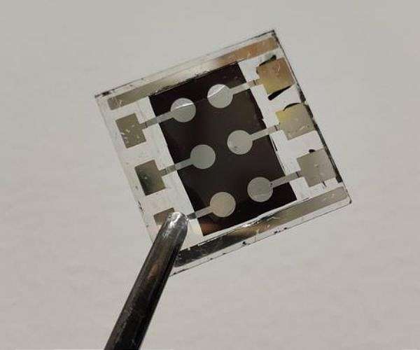
Researchers at the Hefei Institutes of Physical Science of the Chinese Academy of Sciences have engineered an optimized electron transport layer for inverted perovskite solar cells that raises both power conversion efficiency and operational stability. The work, led by Prof. Pan Xu at the Institute of Solid State Physics, focuses on controlling the behavior of the fullerene derivative PCBM at the perovskite interface.
Perovskite solar cells have now reached power conversion efficiencies close to 27 percent, placing them among the leading candidates for next generation photovoltaic technologies. The Hefei team had previously reported a method to homogenize cation distribution within the perovskite absorber, improving that layer’s performance. In parallel with absorber optimization, they note that semiconductive charge transport layers are essential for efficient charge separation and extraction in complete devices.
PCBM, or -phenyl-C61-butyric acid methyl ester, is widely used as an electron transport material in inverted perovskite architectures but tends to form dimers when exposed to heat and light. This dimerization reduces charge carrier mobility, lowers device efficiency, and accelerates performance degradation, which poses a barrier to practical deployment. To understand and mitigate this effect, the researchers examined how PCBM molecules stack on different perovskite surface terminations and identified molecular orientation heterogeneity as a major factor that promotes dimer formation.
Building on this analysis, the team designed a PCBM precursor additive, 2,3,5,6-tetrafluoro-4-iodobenzoic acid (FIBA), to tune the molecular packing at the interface. FIBA interacts with PCBM at the perovskite surface and guides the molecules into a more ordered stacking arrangement, which homogenizes their orientation. This alignment changes the local topology so that the configuration needed for the cycloaddition reaction that produces PCBM dimers is suppressed, thereby inhibiting dimer formation at the transport layer.
Molecular dynamics simulations helped clarify how the additive modifies PCBM stacking and orientation at the microscopic level, linking molecular-scale organization with changes in macroscopic device behavior. The researchers then incorporated the optimized PCBM layer into inverted perovskite solar cells and systematically evaluated photovoltaic performance across different device sizes.
Using this approach, the group reported a power conversion efficiency of 26.6 percent for small-area devices with an active area of about 0.1 square centimeters. Single-cell devices with an area of 1 square centimeter reached 25.3 percent efficiency, while large-area modules covering 762 square centimeters achieved 21.3 percent efficiency. These results indicate that the interfacial strategy can be applied from laboratory-scale cells to larger modules.
The modified transport layer also improved device stability under combined environmental stresses. Optimized cells retained more than 85 percent of their initial efficiency after 2,000 hours of continuous operation under concurrent heat, humidity, and light exposure. The authors conclude that guiding PCBM stacking and suppressing dimerization offers a practical route to simultaneously enhance efficiency and stability in inverted perovskite solar cells and may be applicable to other perovskite-based device structures.
Research Report:Suppression of PCBM dimer formation in inverted perovskite solar cells
Related Links
Hefei Institutes of Physical Science Chinese Academy of Sciences
All About Solar Energy at SolarDaily.com


