by Riko Seibo
Tokyo, Japan (SPX) Dec 17, 2025
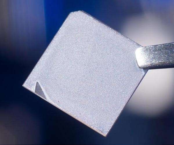
Researchers at Chonnam National University in the Republic of Korea report that a nanometer scale germanium oxide layer can address a longstanding bottleneck in tin monosulfide thin film solar cells by improving the rear contact interface with the metal electrode. They focused on tin monosulfide, or SnS, a non toxic and low cost absorber that uses earth abundant elements and avoids indium, gallium, and tellurium while offering favorable optical and electronic properties for sunlight harvesting in theory. In practice, measured efficiencies have lagged theoretical predictions because of structural defects, parasitic reactions, and atomic diffusion at the interface where SnS meets the back metal contact.
The team led by Professor Jaeyeong Heo and Dr Rahul Kumar Yadav designed a device architecture that inserts an ultra thin germanium oxide, or GeOx, interlayer between the molybdenum back contact and the SnS absorber. Their study, published online in Small on September 19 2025, describes how this interface engineering strategy targets deep level defects and unwanted chemical phases that form during high temperature processing of conventional SnS cells.
To fabricate the GeOx layer, the researchers used a vapor transport deposition process that first deposits a very thin germanium film and then relies on its natural oxidation to form a controlled oxide with a thickness of about 7 nanometers. This approach is compatible with scalable, industry oriented thin film processing. “Despite its nanoscale thickness, this interlayer addresses several long-standing challenges at once,” explains Prof. Heo. “It suppresses harmful deep-level defects, blocks unwanted sodium diffusion, and prevents the formation of resistive molybdenum disulfide phases during high-temperature fabrication.”
By stabilizing the rear interface, the GeOx layer improves the microstructure of the SnS absorber, yielding larger and more uniform grains that facilitate charge transport. The authors report enhanced charge collection and lower electrical losses, which collectively raise the overall device performance. In quantitative terms, the power conversion efficiency increased from 3.71% in standard devices without the interlayer to 4.81% when the optimized GeOx passivation was implemented, one of the highest efficiencies reported for vapor deposited SnS based solar cells.
The work also highlights broader implications of precise control over metal semiconductor interfaces beyond photovoltaic devices. The researchers note that similar interface optimization can influence contact resistance and switching behavior in thin film transistors, energy conversion performance in thermoelectric modules, charge transfer and detection sensitivity in sensors, mechanical reliability in flexible electronics, and operation of photodetectors and memory devices. “Across all these applications, mastering the metal/semiconductor interface remains central to advancing next-generation devices,” says Prof. Heo. “We believe that this work will open new avenues for research, contributing to the development of advanced solar cells and other key technologies.”
Related Links
Chonnam National University
All About Solar Energy at SolarDaily.com


