by Riko Seibo
Tokyo, Japan (SPX) Feb 08, 2026
Researchers from the Qingdao Institute of Bioenergy and Bioprocess Technology (QIBEBT) of the Chinese Academy of Sciences have reported a new interface engineering strategy that significantly boosts the efficiency and stability of three dimensional perovskite solar cells.
Working with international partners, the team formed a thin two dimensional perovskite phase at the buried interface of the perovskite absorber, a location that has been difficult to target selectively with earlier approaches.
The work, published in Nature Energy on February 6, shows that the method improves the crystallization quality of the perovskite films and cuts defect concentrations at buried interfaces by more than 90 percent, a tenfold decrease.
Defects at the top and bottom surfaces of perovskite layers remain a major bottleneck for both photovoltaic performance and long term stability in perovskite solar cells.
One known strategy is to incorporate long chain ammonium salts into the bulk perovskite, which can generate two dimensional perovskite phases in the bulk and at buried interfaces.
However, earlier techniques have struggled to confine these two dimensional structures only to the buried interface, where they can passivate defects without disrupting charge transport in the rest of the absorber.
To overcome this, the QIBEBT led team sequentially grafted thioglycolic acid and oleylamine onto the surface of tin dioxide nanoparticles, producing a modified electron transport material referred to as SnO2-TGA-OAm.
Strong chemical bonding between the thioglycolic acid and oleylamine on the nanoparticle surface controls how the perovskite precursor interacts with the interface during film formation.
During thermal annealing of the perovskite film, cation exchange between the grafted layer and formamidinium iodide proceeds in the solid state, triggering the spontaneous formation of a two dimensional three dimensional perovskite heterostructure only at the bottom interface.
The resulting SnO2-TGA-OAm layer acts as a multifunctional electron transporting layer that both extracts charge carriers efficiently and passivates defects at the buried contact.
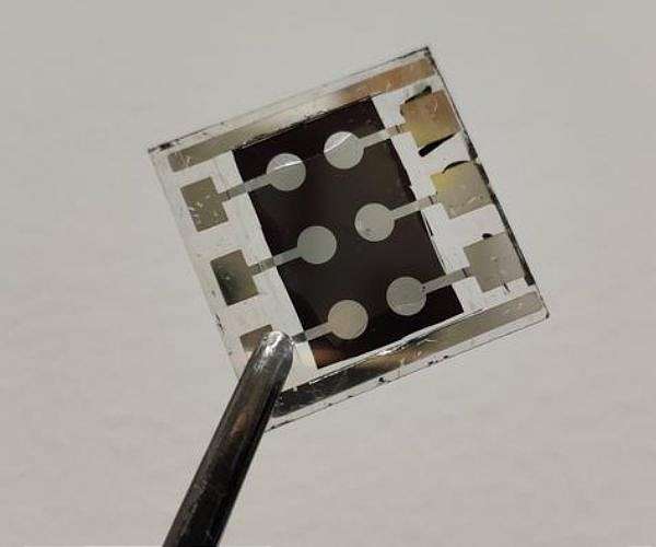
Devices built with this engineered interface achieved power conversion efficiencies of 26.19 percent for small area cells with an active area of 0.09 square centimeters.
The researchers also demonstrated a module with an aperture area of 21.54 square centimeters that reached a power conversion efficiency of 23.44 percent and was certified at 22.68 percent.
In addition, a large area module with an aperture area of 64.80 square centimeters delivered an efficiency of 22.22 percent, underscoring the scalability of the interface design from small cells to modules.
“These values rank among the highest efficiencies reported to date for small sized PSCs and modules based on 2D/3D perovskite heterojunctions,” said first author Dr. Zhao Qiangqiang of QIBEBT.
“This in situ solid state ligand exchange strategy could be easily scalable from lab to factory production while delivering enhanced operational stability,” added corresponding author Prof. Pang Shuping.
According to the team, the combination of high efficiency, reduced interfacial defects, and improved operational stability brings the commercialization of perovskite solar cells closer to reality.
The study demonstrates a general route for fabricating 2D/3D heterojunctions specifically at buried interfaces of perovskite absorbers, a capability that is expected to support further performance gains in perovskite photovoltaic technology.
Research Report:Buried 2D/3D heterojunction in n-i-p perovskite solar cells through solid-state ligand-exchange reaction
Related Links
Qingdao Institute of Bioenergy and Bioprocess Technology
All About Solar Energy at SolarDaily.com


