by Robert Schreiber
Berlin, Germany (SPX) Feb 18, 2026
Despite being riddled with impurities and defects, solution processed lead halide perovskites continue to defy expectations as highly efficient solar cell materials, with performance now approaching that of industry standard silicon based devices. A new experimental study from the Institute of Science and Technology Austria (ISTA) offers a comprehensive physical explanation for this efficiency puzzle and points the way to more effective next generation photovoltaic technologies.
Over the past 15 years, lead halide perovskites have risen from relative obscurity to become leading candidates for low cost, high performance solar cells. Originally catalogued in the 1970s for their hybrid organic inorganic crystal structures and then largely forgotten, these compounds were rediscovered in the early 2010s when researchers found that they exhibit exceptional photovoltaic behavior as well as strong performance in light emitting diodes and X ray detection and imaging.
Perovskites also display striking quantum mechanical properties, including quantum coherence at room temperature, making them attractive testbeds for complex condensed matter physics. Yet their practical promise has been shadowed by a basic paradox. Unlike silicon solar cells, which rely on ultra pure, carefully grown single crystal wafers to minimize defects, perovskite devices are typically made using inexpensive solution based processes that leave them filled with structural imperfections.
In conventional silicon technology, such defects are carefully eliminated because they trap charge carriers and prevent them from traversing the hundreds of microns required to reach the electrodes and generate useful current. The question for perovskites has therefore been how electrons and holes manage to move over long distances and survive for long times in a material that, by standard criteria, should be riddled with traps and recombination centers.
ISTA postdoctoral researcher Dmytro Rak and assistant professor Zhanybek Alpichshev tackled this problem by focusing on how charges behave inside the bulk of a perovskite crystal. Earlier studies had shown that when electrons and holes form tightly bound excitons in these materials, they typically recombine rapidly. Nevertheless, experiments also indicated that in working devices the charges often remain separated for extended periods, an apparent contradiction that suggested some internal force must be acting to pull the pairs apart.
To probe this idea, the team used nonlinear optical methods to inject electrons and holes deep within single crystal perovskite samples and then monitored the resulting electrical response. Each time they generated a fresh population of charges, they detected a finite current flowing in the same direction through the material even though no external voltage was applied. This behavior pointed to built in internal fields capable of separating opposite charges well away from the electrodes.
However, standard characterizations of the intrinsic crystal structure of lead halide perovskites had indicated that such bulk photovoltaic effects should not be present uniformly throughout the material. Rak and Alpichshev proposed instead that the crucial fields reside at domain walls, thin regions of modified structure that form a microscopic network extending through the crystal. At these walls, local distortions could break the symmetry and create strong internal electric fields.
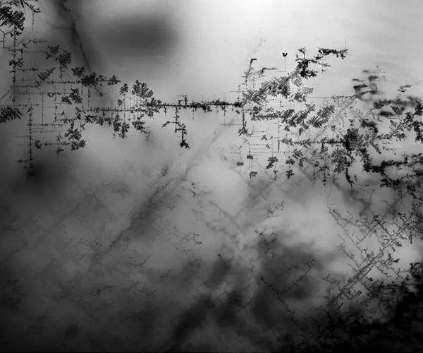
Visualizing such a domain wall network deep inside a crystal posed a major experimental challenge, because many common probes are sensitive mainly to the surface where properties can differ from the bulk. Drawing on his chemistry background, Rak devised an electrochemical staining method that uses ionic conduction in the perovskite to highlight the internal structure. He allowed silver ions to diffuse into the crystal where they preferentially accumulated at domain walls, then converted the ions into metallic silver so that the resulting filaments could be imaged with optical microscopy.
The resulting pictures revealed a dense, sample spanning network of silver enriched paths that trace the domain wall skeleton of the crystal. Alpichshev likens the method to angiography in living tissue, but applied to the microstructure of a solid, because it exposes the internal channels along which charges can move. The qualitative technique, invented and implemented at ISTA, provides direct evidence that perovskites host intricate internal architectures rather than being uniformly disordered.
Rak and colleagues interpret these domain walls as natural highways for charge carriers. When light absorption creates an electron hole pair near one of these walls, the local electric field pulls the negatively charged electron and the positively charged hole to opposite sides, preventing immediate recombination. Once separated, the carriers can drift along the extended domain wall network for distances that would be extraordinary on a microscopic timescale, eventually reaching the electrodes and contributing to the current.
In this picture, the very defects that would be detrimental in a conventional semiconductor become functional elements that enable efficient energy harvesting. Instead of striving for defect free crystals, perovskite technology benefits from the presence and connectivity of flexoelectric domain walls that crisscross the bulk and sustain long range charge transport under illumination.
The authors argue that their framework reconciles a range of previously conflicting experimental observations on lead halide perovskites, including rapid exciton recombination in some measurements and long carrier lifetimes and diffusion lengths in others. By emphasizing the role of internal fields and domain wall networks, their model offers a unified understanding of how these materials achieve high power conversion efficiencies despite apparent structural disorder.
Up to now, much of the research effort in perovskite photovoltaics has centered on adjusting chemical composition to improve stability and performance, often with only incremental gains. The ISTA findings suggest a complementary path that focuses on engineering the density, orientation and connectivity of domain walls to optimize charge separation and transport while preserving the solution based, low cost fabrication routes that make perovskites attractive for large scale deployment.
Research Report:Flexoelectric domain walls enable charge separation and transport in cubic perovskites
Related Links
Alpichshev Group at Institute of Science and Technology Austria
All About Solar Energy at SolarDaily.com


